215.631.7111

S-BOND BLOG

Sensors and Actuators

Sensors and actuators are a growing commercial market with the Internet of Things (IOT) and the interest to remotely monitor and control many devices.

S-Bond® active solders are finding more application in sensors and actuator devices due to their use of dissimilar materials, including metals, intermetallics, ceramics, composites and glasses which need to be joined. S-Bond® active solders are unique in that they can join such materials, without flux or plating, at low temperatures and with excellent conductivity (both electrical and thermal).

S-Bond® active solders can bond…

  • All metals (Al, Cu, St. Steel, Ti, W, Mo, Ni, etc)
  • Ceramics (Al2O3, SiO2, Sapphire, Quartz, Zirconia, AlN, Si3N4, etc)
  • Carbon / Carbides (SiC, TiC, WC, Graphite, Diamond, etc)

With Ce, Ga and Ti additions to solder filler metals, S-Bond® solders can bond direct to oxides, nitrides and carbides that have formed on metal surfaces, directly. On aluminum and copper the Ga and Ce interact with the oxides that form on these metals then the Sn and Ag constituents form metallurgical intermetallic compounds (IMC’s) that chemically bind the solder to the aluminum or copper base metal. With the active S-Bond® solders’ ability to wet, adhere and join such a diverse set of materials, the S-Bond® alloys find wide application in sensors and actuators that employ a diverse array of materials and in dissimilar material joints… These joints have many requirements, depending on the application, these requirements include…

  1. Thermally conductive
  2. Electrically conductive
  3. Transmits sound
  4. Hermetically seals
  5. Bond strengths high enough for the application
  6. Low temperature joining
  7. Accommodation of CTE mismatch strain

Sensors and Actuators that S-Bond® is currently specified in includes…

Piezo ceramic (PZT) – Ultrasonic Gas Flow sensors; PZT ceramic disks are S-Bond® soldered to stainless steel housings that transmit and receive u/s sound pressure waves. The transmit sensor with bonded PZT piezo ceramic disk sends u/s waves into a passing gas flow and a receive sensor with bonded PZT receives and converts the sound waves… with a shift in frequency known as the Doppler effect, can relate the frequency shift to the mass flow of the passing gas stream. In these sensors, the piezo ceramic disk needs to be intimately bonded with no voids to create an acoustically “hard” transmitting bond interface, joining the ceramic to metal below the curie temperatures of 250 C.  S-Bond® 220 alloys are being used to make these reliable and acoustically sound interfaces.

MEMS Pressure Gages; Silicon based MEMS devices us Si-dies and incorporate circuitry to use the Si as part of the measurement. In the case of pressure measurements, thin diaphragms of Si are created and strain gage circuitry is deposited using lithography to complete the sensor… the challenge then was so seal the Si-sensor die to a metallic pressure housing that is installed onto the component needing a pressure sensor. S-Bond® active solders can join Si direct to metals and can create a hermetic joint, creating a seal between the Si-MEMS pressure sensor and the mounting housing.

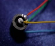
Graphite Electrodes / Water Conductivity Sensors; S-Bond® active solders are being used to join graphite to electrical leads for use in Anode/Cathode systems for making excellent electrical solder connections with the use of flux or pre-plating.


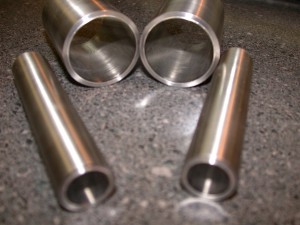
Sapphire – Optical Sensors; Sapphire is single crystal aluminum oxide that is very hard/scratch resistant and also transits optical signals in a specific spectrum. As sapphire is an excellent “window” material for many optical signals. For example in Gamma Ray Detection, NaCl single crystal creates photon (light) output proportional to the impinging gamma ray radiation intensity.  The NaCl crystal will degrade/dissolve in contact with air, to the crystal is housed behind a sapphire window which is S-Bond® active solder sealed (hermetic/He leak free) to a titanium tube to create a sealed environment that the gamma rays can penetrate. Optical detectors are then mounted in front of the sapphire window, outside the S-Bond® sealed enclosure.

Insulators /Radar Sensors; Printed 3-D circuits are being made to generate / receive radar signals.  These circuits are built through ceramic layers that form a ceramic backbone to the sensors’ circuitry. S-Bond® active solders have been used to bond the edges of this ceramic backbone of the sensor and seals it from the environment.

Magnet Assemby – Actuators; Magnetic actuators are used to move valves, switches and other devices dependent on precise and reliable stroke based motion. Such magnetic actuators are using high force as CoSm based magnets. These magnets will form a strong and specific magnet fields. In one actuator design, the actuator “rod” runs on the magnet assemblies’ magnetic axis. To assure optimal actuator lineal translation, the actuator’s central push rod could not be magnetic, so it a ceramic rod was selected. In this actuator, S-Bond® active solders have been used to bond the central ceramic rod to the magnetic core of the actuator.

As presented here, S-Bond® solders are being applied in a growing range of sensors and actuators. If you would like to take advantage of S-Bond® solders unique capabilities to join dissimilar materials in your sensors and actuators, please Contact Us.

Joining Thermal Management Graphite Composites

S-Bond® active solders enable graphite bonding and the joining of other carbon based materials to each other and to most metals within the constraints of thermal expansion mismatch. S-Bond® alloys have active elements such as titanium and cerium added to Sn-Ag, Sn-In-Ag, and Sn-Bi alloys to create a solder that can be reacted directly with the carbon surfaces prior to bonding using specialized S-Bond® treatments for solder joining. Reliable joints have been made between graphite and carbon based materials with all metals including steel, stainless steels, titanium, nickel alloys, copper and aluminum alloys.

In high power density electronics, there is a need to rapidly spread and dissipate heat generated by the high frequency operations in the electronics.  In order to improve the heat dissipation capacity of graphite based materials, Applied Nanotech developed a new passive thermal management material, CarbAl™, which is a carbon-based material with a unique combination of low density, high thermal diffusivity, and low coefficient of thermal expansion based on Figure 1.

Figure 1. Picture of the CarbAl-G high thermal diffusivity graphite composite.

Applied Nanotech reports that CarbAl™ has a density of 1.75 g/cmcompared to 2.7 g/cmfor aluminum and 8.9 g/cmfor copper. While copper has a slightly higher thermal conductivity than CarbAl™, 390 W/mK compared to 350 W/mK, CarbAl’s thermal diffusivity is approximately 2.9 cm2/sec compared to 0.84 cm2/sec for aluminum and 1.12 cm2/sec for copper.

S-Bond Technologies and Applied Nanotech have collaborated to make heat spreaders with CarbAl-G cores combined with copper and aluminum claddings to make the heat spreaders that are more robust and able to be fabricated to support a high density of high power electronic devices, yet be mounted in standard “PC” card configurations as seen in Figure 2.

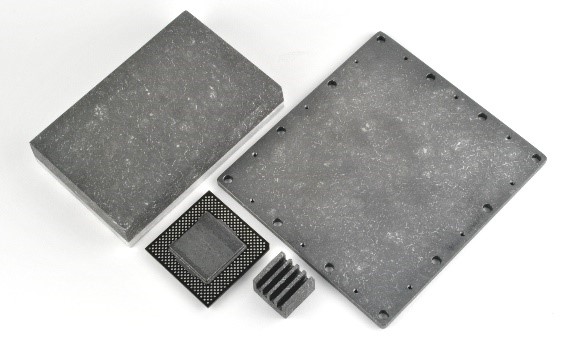
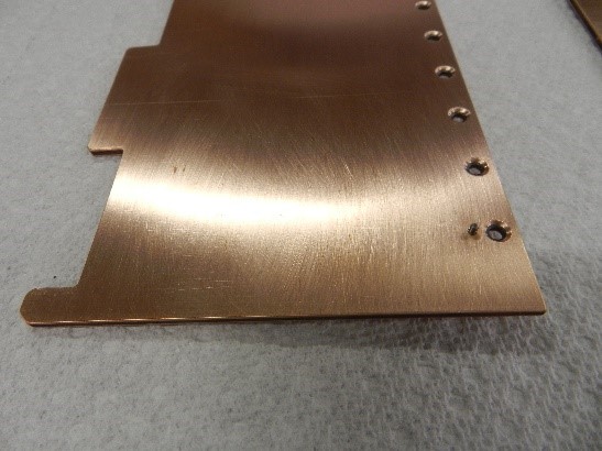
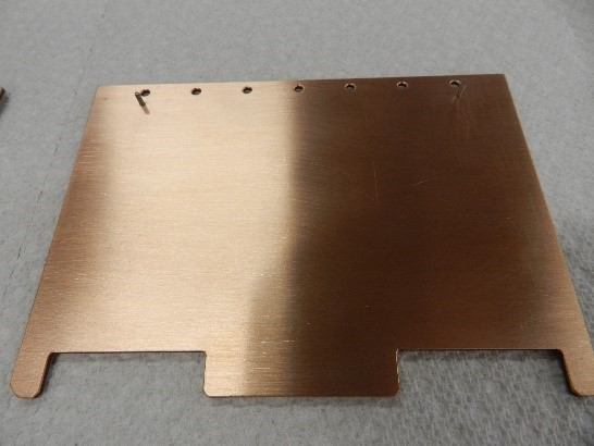
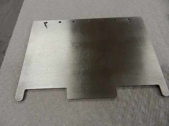
Figure 2. Copper and Aluminum clad CarbAl-G circuit boards.

These clad CarbAl-G cored boards have utilized active S-Bond® solder layers to intimately bond and thermally connect the thin copper or aluminum claddings to the lightweight, high thermal diffusivity CarbAl-G composite sheets.

S-Bond® CarbAl-G bonding and joining was thermally activated using S-Bond Technologies proprietary process, which prepared the CarbAl-G surfaces and developed a chemical bond to the surface, through reactions of the active elements in S-Bond® alloy to the graphite in CarbAl-G. These joints start with processing the graphite/carbon surfaces at elevated temperatures in a protective atmosphere furnace with S-Bond® alloy placed on the graphite-carbon surfaces to be joined. At these elevated temperatures, the active elements in S-Bond® (Ti, Ce, etc.) react with the ceramic to develop a chemical bond. After the CarbAl-G is prepared / S-Bond® metallized, the CarbAl-G is then S-Bond® soldered to the aluminum or copper sheets to for a metal clad CarbAl-G composite plate that can then be machined into a heat sink plate to which high power electronic devices be mounted.

The S-Bond® solder joints produced:

  • Are ductile, based on Sn-Ag or Sn-In alloys
  • Exceed the strength of the CarbAl-G
  • Are thermally conductive, with S-Bond® alloys having k = 50 W/(m-K)
  • Are metallic and this electrically conductive with a metallurgical bond

S-Bond Technologies has developed extensive experience in active, S-Bond® solder joining of graphite, carbon and carbide to metals. Contact Us to evaluate our joining solutions for your graphite joining applications. For more information on CarbAl-G, please contact Applied Nanotech. Inc

Bonding Graphite Felts To Metals

Graphite and carbon felts are increasingly being used for applications in solar, LED, medical, semiconductor, automotive and energy storage systems.

S-Bond Technologies (SBT) has customized it S-Bond (S-B) processes to bond graphite felts to metals for such applications. In the process, graphite felts are first S-B metallized using a paste and vacuum process to create a metallurgical bond between graphite and the SBT active solder filler metals. After S-B metalizing of the graphite, only the tips of the felt surfaces are metallized and thus solderable to the opposing metal plates that are coated with SBT active solders.  The S-B metallization process does not fill the open cells of the graphite felts with S-B alloys, hence its advantage for bonding open cell structures.
(more…)

Design Considerations for Solder Bonding

Solder bonding is a versatile lower temperature bonding process that is used in joining a range of metals, ceramics, glass and metal: ceramic composites. By definition, solders are joining filler metals that melt below 450°C. Solder bonding is typically used in the assembly of structures for its good thermal and/or electrical contact or for creating seals. The advantage of solder bonding stems from lower temperature exposure (less that 400°C), compared to brazing when joining thermally sensitive materials.  Alternatively, compared to bonding with epoxy adhesives, solder bonding is a more conductive bond, but does require higher temperature exposure and the wetting of the molten metal to the bonding surfaces.

Figure 1. S-Bond joined heat pipe assembly bonding copper pipes to aluminum base

Because of it excellent thermal and electrical conductivity, solder bonding finds application in the manufacture of sputter targets, heat spreaders and cold plates and other related thermal management components. Solder bonding is also used to seal ceramic:metal and glass windows used in optical based sensors and in other fluid cooled enclosures.  Figures 1 and 2 show several typical solder bonded parts.

Solder bonding (e.g. S-Bond®), despite being versatile and capable of joining most materials, one must consider several issues when active solder bonding…

  • Thermal expansion mismatch
  • Size and shape of bonded parts
  • Interaction with post solder bond processing
  • Galvanic corrosion coupling
Figure 2. Aluminum to copper cooling tubes and ceramic to plated copper sputter targets.

In every application being evaluated for a solder bonding solution, the component and process design needs to consider the following issues.

  • Minimize CTE mismatch of bonded materials to prevent distortion or fracture.
  • Understand post bonding processes to prevent damage of bond interface.
  • Know Service Temperature and Thermal cycling effects on bond interface.
  • Understand effects of service environment on bond interface corrosion

Thermal expansion mismatch (CTE): solder bonding requires heating the component parts in an assembly to 120 – 400°C, depending on the solder filler metal being used.  When similar materials are being joined there is no CTE mismatch so it is not a concern. However; many times solder bonding is being used to lower the CTE mismatch… but despite the lower bonding temperature, it is not alone a “silver bullet” universal solution. Even when heating to 250°C, melting for Sn-Ag based solders, upon cooling once the solder solidifies it can transfer a strain. Then the CTE derived stresses can distort metal assemblies, fracture a glass or ceramic components or fracture the bond. Thus, one needs to minimize CTE mismatch stresses by selecting assemble component materials that are as close as possible in CTE.

When matching CTE is not practical, then one should design the component parts with size and thickness in mind… larger bond areas will “accumulate” more stress and lead to more distortion and/or fracture. A solution for larger parts is to “tile” the component parts; by tiling (mosaic) the strain mismatch accumulation is interrupted and lower the accumulation of stress in the assembly.

Post solder bond processes such as post solder bond heating either with another solder process, welding or bake outs to dry or cure components. Coatings may also be required on a bonded assembly where the heat and or chemical exposure of the coating process, as in electro-plating (see the coating blog article), interacts negatively with the solder bond.

When post processing a solder bonded part, temperature exposures typically should be below 90% of the solidus temperature (temperatures where solder alloys begin to melt) to maintain the bond. The thermal cycle itself can be damaging to the bond, even if the temperature is below this limit, especially with assemblies that have dissimilar materials. The processes that can degrade solder bonds include, other solder steps, welding, bake out or curing, and coating. Therefore; one needs to understand their impact on the solder filler metals and the solder bond interface.

Service conditions can also limit the performance and life of solder bonds. Temperature in service generally needs to be restricted to be below 80% of the solidus temperature of the solder filler metal (although active solders such as S-Bond® can be used up to 90%) to maintain sufficient bond strength. Thermal cycles are more damaging than constant temperature exposure and can be more damaging when CTE mismatched materials. Joint design can mitigate some of these effects by…

  • Selecting component materials to lower CTE mismatch
  • Minimizing area of solder bond and consider tiling, if practical
  • Using thicker cross sections, if possible,  to limit distortion
  • Orienting or mechanically supporting solder bonds/seals to lower bond stresses.

With proper design solder bonded assemblies can be superior to epoxy bonded joints and work very well and compete with brazed or welded joints

Contact us for more information and to order our S-Bond products and Services.

Joining Dissimilar Materials

The Issue of Coefficient of Thermal Expansion (CTE) Mismatch

Yes, S-Bond can join a wide variety of materials, including aluminum, copper, stainless steel, refractory metals and ceramic to metal brazing with aluminum oxide, aluminum nitride, silicon carbide and other oxide, nitrides and carbides… however, with this wide variety of materials joining capability, we have a lot of inquiries about aluminum soldering to stainless steel or aluminum oxide, graphite bonding to aluminum, titanium to silicon carbide, etc. (more…)