ULA has recognized S-Bond Technologies with a Small Business Excellence Award for their support of the Vulcan Centaur program. As a materials technology company that provides bonding solutions for a broad range of materials, S-Bond played an integral role in providing its active solder technology in the Vulcan Soldered Transition Ring qualification.
Launch of Atlas V Juno from Cape Canaveral AFS
S-Bond active solders were instrumental in providing a seal for the Transition ring that feeds liquid oxygen into Vulcan Centaur’s main engine. These seals have undergone rigorous cryogenic testing resulting in ULA’s use of this technology.
Contact Us for more information on how S-Bond solders can solve your bonding challenge.
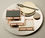
S-Bond Technologies’ active solders are finding wide application in semiconductor processing equipment. Their capability to join a wide range of dissimilar materials and the fact that as a filler metal, their bonds are thermally conductive make S-Bond solders far superior to many other commercial bonding/thermal interface materials. Semiconductor processing applications include…
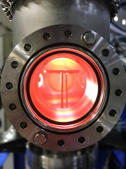
In sputter targets, the deposition/target materials is sputtered (high energy ion impacts displace a target’s atoms) onto an opposite surface to form a functional coating or other element layer in a computer chip, TV screen or other semiconductor device. The high energy impact of the deposited films require “sputter targets” to be cooled to keep the target material layer from melting. To cool the target, water is circulated in an aluminum or copper base plate. S-Bond active solders can bond all metals and most ceramics that are commercially used to produce sputtered films. Active solders can bond these sputter targets to either Copper or Aluminum, bonding them at low temperatures (which minimizes thermal expansion mismatch stresses), without flux contamination/entrapment (which will contaminate the sputtering plasma), and with excellent thermal conductivity (a metallic bond with nearly no voids).
For probes and sensors, S-Bond active solders can bond silicon or carbide/carbon based devices (MEMS or other semiconductor based probes) directly to metal and metallic conductor leads. The low temperature active solders, when joining semi-conductor devices, impart low residual stresses and the joints are electrically and thermally conductive… good for signal transmittance and cooling.
Piezoceramics such as Pb-Zirconates (PZT) that impart force/small displacement or create ultrasonic pulses, can be bonded direct to metals with active solders. Bonding is accomplished bonded below their curie points with acoustically sound interfaces that can transmit sound effectively. Such piezoceramic based sensors and actuators are used in accurately measuring gas flow and can be used on gas control in MOCVD processes used to deposit and etch computer chips. S-Bond active solders can wet and adhere to most piezoceramics all without pre-plating and chemical fluxes… as such they are finding excellent application in probes and sensors used on semiconductor processing.
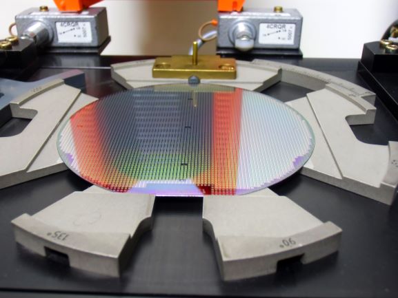
Wafers (silicon or other) are placed into energetic plasmas and other beams to deposit then etch a complicated surface morphology in layers to create semiconductor based chips. The high heat energy into the wafer needs to be removed through water cooled wafer handling devices such as the pedestals the wafer sits on in their processing chambers. If not cooled, the interdiffusion of the fabricated on the wafer. With the latest 300mm diameter wafer technology over a $1M work of chips can be on a wafer.
The high energy levels used in semiconductor processing requires well cooled and reliable handling equipment. S-Bond active solders can intimately join copper and aluminum as well as other thermal management materials such as AlSiC and pyrolytic graphite.
If you would like to see how S-Bond active solders can improve your semiconductor processes and handling and measuring equipment, please Contact US.
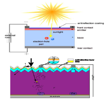
In recent years, active solders have made their way into use in solar panel manufacture. To understand where S-Bond solder alloys are being used one has to understand the solar panel construction. Solar panels consist of arrays of solar cells, soldered together. A solar cell consists of three basic elements, top contact, base and rear contact, as shown in Figure 1. From the back of each solar cell, electrical contact needs to be made between these surfaces to close the circuit and provide an electron path as photons emit electrons in the semiconductor polysilicon photovolatic (PV) cell which migrate to the back of the exposed cell surface, as illustrated.
Carrying water to the space station is a real challenge and cost, hence recycling water is critical. Waste water, sweat and other ISS water is constantly recycled in a complex system that evaporates and condenses clean water for reuse. For more information on the space station recycling system see the following link: Water Recovery System.
While it has been several years since manufacturers began moving to lead-free solder procedures, in part due to the European Union’s Restriction of Hazardous Substances Directive, some still believe myths that have long been inaccurate regarding the use of alloy joining materials that do not require flux and are based on lead and tin.
Temperatures Can Be Enough to Destroy Components
The first round of lead-free solder options to join metals and other materials were comprised of tin, silver and copper, which do have a slightly higher melting point of 217 degrees Celsius compared to existing solder’s 183 degrees Celsius. That disparity could cause problems regarding PC board damage.
However, newer products including several offered by S-Bond have significantly lower melting points that make it easier to join metals like aluminum. At the lowest temperatures, some materials can be joined at just 115 degrees Celsius.
Issues Regarding Silicon Will Require Other Materials
Thermal interface materials are materials used in creating heat conductive paths at interfaces between components and thus reduce thermal interface resistance. These materials permit more effective heat flow between separate components where heat is being generated to a heat dissipation components such as solid state transistors to heat sink or a high frequency device connected to a heat spreader. Thermal interface materials’ purpose is to fill the air gap that occurs at contact interfaces with more thermally conductive compounds to permit more effective heat flow than poorly conductive air.
There is a wide variety of thermal interface materials (TIM’s); thermal greases, phase change polymers, thermal tapes, gap filling pads, filled epoxies and solders. All having various costs, performance and manufacturing challenges.
Figure 1. Illustration of thermal grease filling an interface between a heat generating device and a heat sink.
Thermal greases are viscous fluid substance which increase the thermal conductivity of a thermal interface “gap by filling microscopic air-gaps present due to the imperfectly flat and smooth surfaces of the components as seen in Figure 1.
Thermal grease compounds have far greater thermal conductivity than air (but far less than metals). They are used in electronics, as depicted in Figure 2, to improve the heat flow from lower power electronic devices thus lowering the components temperature and increasing its life.
S-Bond Technologies has developed and proven a new, lower temperature active solder that melts from 135 – 140°C. The solder, S-Bond® 140 is based around the Bismuth-Tin (Bi-Sn) eutectic composition. This new solder is a lower temperature active solder that enables multi-step soldering where previously soldered connections/seals are not remelted. Active solders that melt below 150C are also finding use in thermally sensitive applications where Sn-Ag based solders that melt over 215°C can thermally degrade the component parts being assembled. Lower temperature soldering also can more effectively bond dissimilar materials where thermal expansion mismatch many times fractures or distorts an assembly’s component parts.
S-Bond 140 is already finding application in glass-metal seals in electronic packages where higher temperature soldering alloys would have damaged the packages’ components. S-Bond 140 is also being used to bond heat pipes and vapor chamber thermal management devices to protect the thermally sensitive phase change fluids from damaging the devices when solder bonding to electronic and LED devices.
Electro-optical package to be bonded to heat sink with S-Bond® 140
Mechanical vs Chemical Fluxing During Solder Bonding
Flux is derived from Latin word fluxus meaning “flow.” In solder joining (also aluminum soldering, graphite bonding, ceramic to metal brazing, etc.), a flux facilitates wetting by molten metals disrupting oxides on metal surfaces which interrupt the reaction/interaction of the molten solder metals with the underlying metal. Additionally, flux allows solder to flow easily on the working piece rather than forming beads as it would otherwise. (more…)

 In sputter targets, the deposition/target materials is sputtered (high energy ion impacts displace a target’s atoms) onto an opposite surface to form a functional coating or other element layer in a computer chip, TV screen or other semiconductor device. The high energy impact of the deposited films require “sputter targets” to be cooled to keep the target material layer from melting. To cool the target, water is circulated in an aluminum or copper base plate. S-Bond active solders can bond all metals and most ceramics that are commercially used to produce sputtered films. Active solders can bond these sputter targets to either Copper or Aluminum, bonding them at low temperatures (which minimizes thermal expansion mismatch stresses), without flux contamination/entrapment (which will contaminate the sputtering plasma), and with excellent thermal conductivity (a metallic bond with nearly no voids).
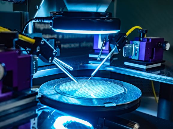 For probes and sensors, S-Bond active solders can bond silicon or carbide/carbon based devices (MEMS or other semiconductor based probes) directly to metal and metallic conductor leads. The low temperature active solders, when joining semi-conductor devices, impart low residual stresses and the joints are electrically and thermally conductive… good for signal transmittance and cooling.