215.631.7111

S-BOND BLOG

S-Bond® Active Soldering of High Purity Fused Silica for Optical Devices

S-Bond®  Ultrasonic Active Soldering of Silica

Ronald Smith    S-Bond Technologies Inc., Hatfield, PA,

Lawrence W. Shacklette, Michael R. Lange, James C. Beachboard,
Harris Corp., Melbourne, FL

and Donna L. Gerrity     E&S Consulting Inc., St. Augustine, FL

Packaging of optical devices often requires the need for creating strong bonds between metal and silica. The most convenient and cost effective approach would be to directly solder to both silica and metal without requiring pre-metallization of the silica. Soldering to oxides and oxidized surfaces has been accomplished with various solders containing metals with strong affinity for oxygen, known as “active solders”.

S-Bond Technologies worked with Harris Corporation to understand S-Bond® 140 active solders, based upon a tin-bismuth eutectic with activating additives of cerium, gallium, and titanium, to produce seals between metals and silica. Titanium and cerium are energetically capable of competing for the oxygen in silica, and are therefore capable of reducing or forming mixed oxides with silica under appropriate conditions. The bond between such an “activated” solder and high purity fused silica (HPFS) has been characterized by Time-of-Flight Secondary Ion Mass Spectrometry (TOF-SIMS). Two variations of solder produced by S-Bond Technologies, S-Bond®140 and S-Bond®140 M1 were bonded to silica using a fluxless ultrasonic technique.

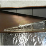
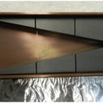
Figure 1 illustrates the ultrasonic soldering process where the resultant cavitation of the molten solder layer continually disrupts the oxides forming on the molten solder surface, enable the active elements to be in direct contact with the base materials own oxide surface, in this case silica, SiO2.

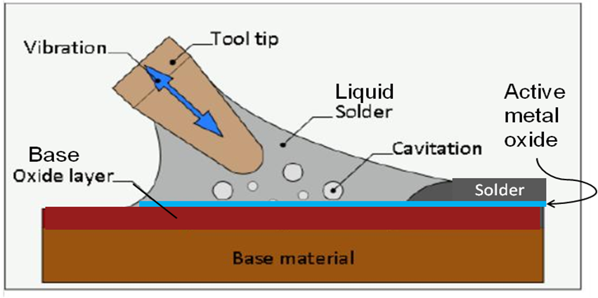
Figure 1. Illustration of ultrasonic soldering process with active solders.

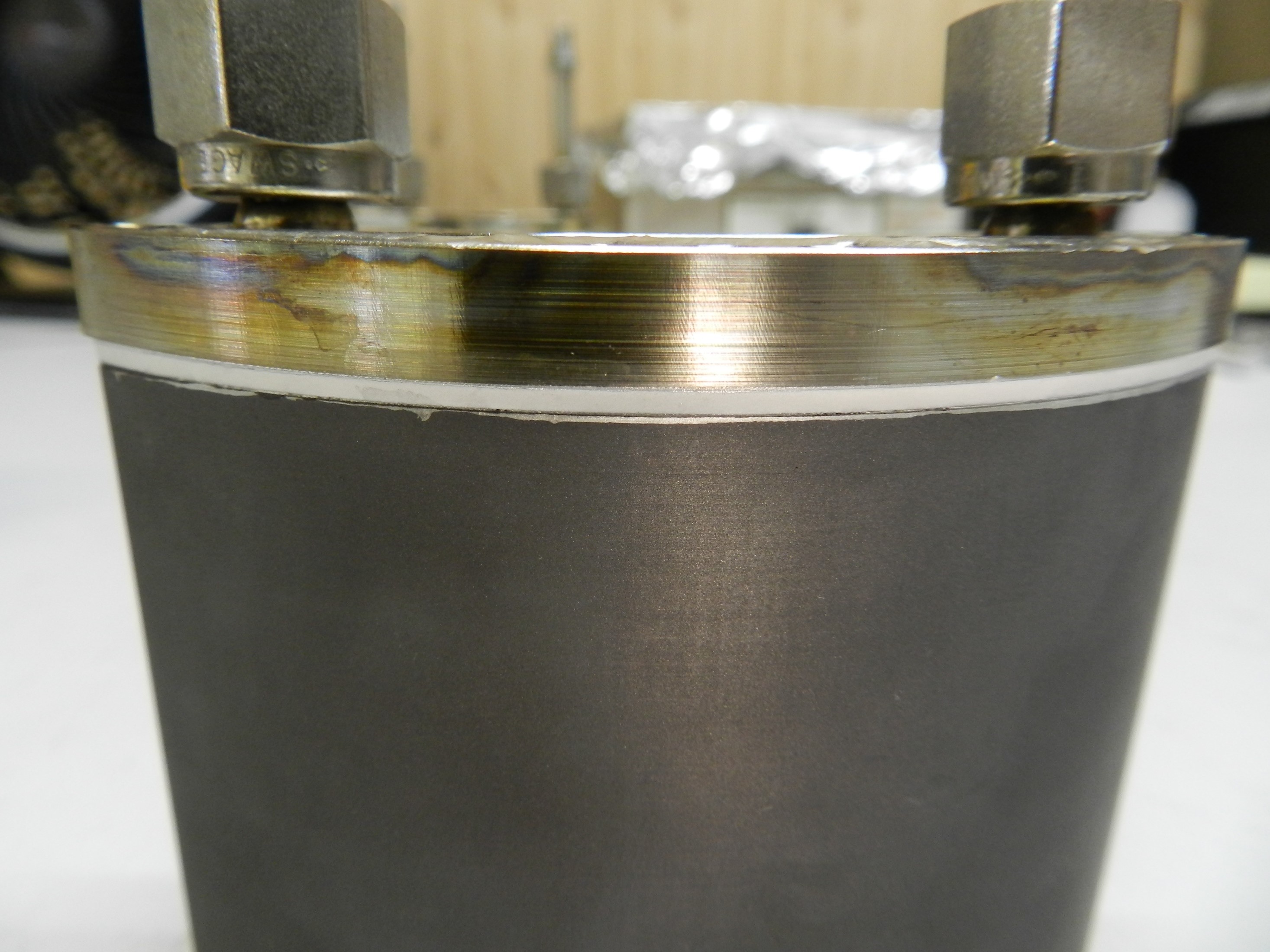
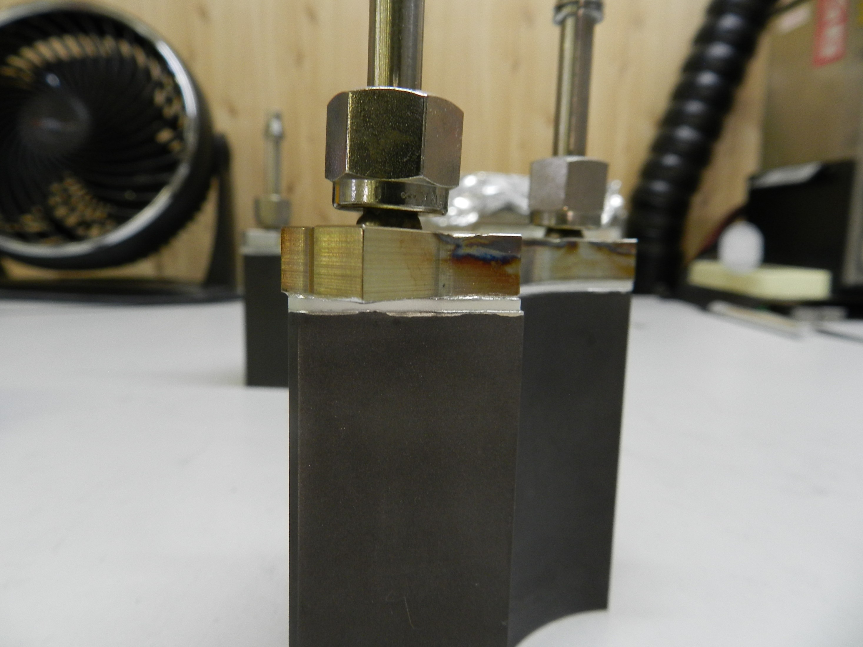
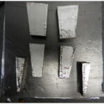
To compare the influence of the active elements on the strength of the soldered bond silica to metal interfaces when using non-activated solders and active solders, a simple overlap soldered coupon ( ~ 1” x 1” ) was used on a compression lap shear test. Figure 2 illustrates the soldered specimen shear test configuration.

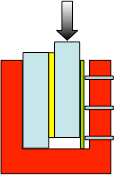
Figure 2. Illustration of compression lap shear test configuration.

Table 1 summarizes the lap shear strengths of the active S-Bond® 140 M1 and compares its shear strength to hose of typical non-active element solders.

Table 1. Compression Lap Shear Test Results

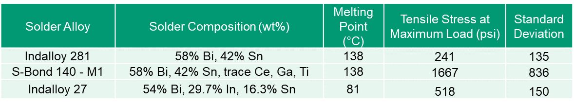
The results in Table 1 show that the active S-Bond® 140M1 solders far exceed the shear strengths of non-active elements solders.

To characterize how the active elements are increasing the bond silica-metal joint strengths, Time of Flight – Secondary-ion mass spectrometry [TOF-SIMS] was used to characterize the bond interface. TOF-SIMS measured the distribution of the various S-Bond® elements as a function of depth through the interface. The results show that the activating elements (Ti, Ce, Ga) concentrate at the interface and that their oxides form the interfacial layer between the high purity silica (HPS) and the bulk solder.

The efficacy of these additives was established by demonstrating that the block shear strength of the bond to HFPS was increased by 7 times through the addition of the Ti, Ce and Ga reactive metals to the base Sn-Bi solder.

The resultant data from the investigation showed a significant increase in the concentration of all of the “active” elements present in S-Bond® 140 M1 within a 220 nm interfacial zone between the solder and HPFS.

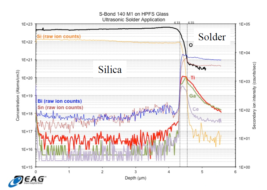
Figure 3. Charts of Element concentrations made from S-Bond® 140M1 joints between Silica and metal using Time of Flight – Secondary-ion mass spectrometry [TOF-SIMS].

In addition to this accumulation of “active” elements, the quantitative concentration of O was higher in the interfacial region than in areas away from the interface in the solder bulk.  These data support the formation of mixed oxides at the interface play a significant role in adhesion.  The data also support the notion that the interface comprises an oxide to oxide bond, that is, a silica to active metal oxide bond. All three active elements present in the solder seem to participate relatively equally in this bond formation.

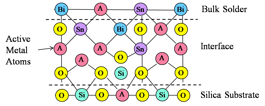
Figure 4. Illustration of mixed oxide bond interface at S-Bond® 140M1 solder to silica surface.

It cannot be necessarily concluded that each active element (Ti, Ce or Ga) has the same contribution to bond strength, or whether having an intermetallic mixed oxide offers an advantage over a simple oxide of a rare earth or titanium.  Based on concentration alone, it appears that the role played by all three metals is essentially the same.  The thickness of the oxide layer (220 nm) and the observation of an interface layer with mixed oxides supports the model depicted in Figure 4.

The active elements accumulate at the interface because this is the available reaction site due to the presence of the substrate oxide (silica) and potential free oxygen. Once the oxidation reaction occurs, the active metal becomes bound at the interface, and thus accumulates there. The mechanism for movement of the “active” elements to the interfacial region against an apparent concentration gradient is presumably due to mechanical forces, but could also be aided by thermal convection.  The ultrasonic energy applied to the system is believed to play a key role in the observed movement of “active” elements to the interfacial region and possibly to an enhanced O level in this same region.  Ultrasonic or any other form of mechanical agitation can establish a mixing of the solder that would bring active metal to the interface.

REFERENCES

[1]          Nagono, K., Nomaki, K., and Saoyama, Y., US Pat. 3,949,118.

[2]          Ramirez, A.G., Mavoori, H. and Jin, S., “Bonding nature of rare-earth-containing lead-free solders”, Appl. Phys. Lett. 80, 3 21, 398-400: and US Pat. 6,306,516.

[3]          Tomáš Skála, Nataliya Tsud, Kevin C. Prince and Vladimír Matolín, “Bimetallic bonding and mixed oxide formation in the Ga–Pd–CeO2 system”, J. Appl. Phys. 110, 043726 (2011).

[4]          A.R. Lobato, S. Lanfredi, J.F. Carvalho, A.C. Hernandes, “Synthesis, Crystal Growth and Characterization of g-Phase Bismuth Titanium Oxide with Gallium”, Mat. Res. vol.3 n.3 São Carlos July 2000.

This investigation has shown how effective active element solders, such as S-Bond 140M1 are in bonding metals to silica (SiO2) surfaces. If you have applications requiring the bonding and sealing of fused silica or related glasses, please Contact Us… and we can assist in meeting your need.

Bonding Graphite –Ceramic – Stainless Steel Composite Component For Los Alamos National Laboratories

Fabricating Parts for Proton Collimator With S-Bond® Active Solders®
The unique capability of S-Bond solders to join graphite and ceramic to metals was the solution for Los Alamos for fabricating core elements of their Proton Collimator used in its Proton Radiography facility. Conventional brazing was considered but their large differences in Coefficient of Thermal Expansions (CTE’s) limited brazing since on cooling from brazing temperatures (over 800°C), the resultant CTE derived residual stresses would have likely cracked the ceramic, graphite or torn the bond interface. Figure 1 illustrates the graphite – ceramic-stainless steel composite assembly that required stable, thermally and electrical conductive connection between the assembly’s elements.

Los Alamos researchers reached out to S-Bond Technologies to use its S-Bond solders to join these disparate materials. Normally plating would have to be used to make the ceramic and graphite materials solderable. In the case of S-Bond joining, the same solder and soldering process was used to make the joint between the graphite base, the insulating alumina sheet and the stainless steel plate, as depicted in Figure 1.

Figure1AProtonColimator

Figure 1. Illustration of the proton collimator elements joined with S-Bond solders.

The soldering of this composite started the S-Bond metallization of the bonding surfaces of the graphite base and the alumina insulator. In this process, S-Bond metallization paste was applied to the one surface of the graphite and the two opposite sides of the alumina paste. The graphite and the alumina sheet with pastes applied, were heated to 960C in a vacuum furnace in order to react the elements in the paste with the graphite and ceramic surfaces to create a chemical bond between the solder and the graphite and alumina.  After metallization these parts’ surfaces are solderable with a well bonded interface. The Graphite base, the alumina insulator plate and the stainless steel header were heated to 250C where S-Bond 220 solder filler metal was applied via melting on and mechanical activation (spreading by heated blade or bush) to pre-tin the faying surfaces of the assembly. Once the S-Bond solder filler metal was pre-placed (pre-tinned) the parts kept hot at 250C, were placed together in an alignment fixture to align the constituent parts accurately and then pressed / loaded with 50 lbs of deadweight as the bonded assembly was cooled.

Figures 2 illustrates the solder bonded composite proton beam collimator component. The pictures show the two S-Bond solder interfaces connecting the water cooled Stainless steel end plate, to the ceramic insulator plate, then connected to the graphite cathode.

Figure2aProtonColimatorFigure 2a. Back of S-Bond joined collimator part. Stainless Steel/ceramic insulator/graphite base (from Top to Bottom)

Figure2bProtonColimatorFigure 2b. Side view of S-Bond joined collimator part.

Figure 3 illustrates the Proton Collimator with the S-Bond joined parts being assembled at Los Alamos National Laboratory (LANL). There were two S-Bond joined parts per assembly. These bonded component assemblies worked very well and enables LANL engineers to successfully implement their design.

Figure3ProtonColimator

Figure 3. Proton Collimator with two S-Bond joined composite being mounted.

LANL engineers were able to utilize S-Bond’s unique capability to solder join stainless steel to ceramic to graphite. If you have such joining challenges, Contact Us for incorporating S-Bond joining in your assemblies.


Myths Regarding Lead-Free Solder Products and Joining Techniques

Soldering Techniques - Joing Methods
Brush Application

While it has been several years since manufacturers began moving to lead-free solder procedures, in part due to the European Union’s Restriction of Hazardous Substances Directive, some still believe myths that have long been inaccurate regarding the use of alloy joining materials that do not require flux and are based on lead and tin.

Temperatures Can Be Enough to Destroy Components

The first round of lead-free solder options to join metals and other materials were comprised of tin, silver and copper, which do have a slightly higher melting point of 217 degrees Celsius compared to existing solder’s 183 degrees Celsius. That disparity could cause problems regarding PC board damage.

However, newer products including several offered by S-Bond have significantly lower melting points that make it easier to join metals like aluminum. At the lowest temperatures, some materials can be joined at just 115 degrees Celsius.

Issues Regarding Silicon Will Require Other Materials

(more…)

S-Bond Joining of SiC Tiles in Microwave Beam Dampers (Absorbers)

Argonne National Laboratories selected S-Bond active solder technology to make water cooled high power microwave beam dump in its Advanced Photon Source which is a user-facility to producing extremely brilliant x-ray photon beams. The Advanced Photon Source uses high energy microwave beams to steer and create such x-ray photon beams. These beams once started cannot be shut down or restarted easily, so to facilitate the use the various beam lines, the microwave beams are diverted to beam dumps. These beam dumps consist of microwave cavities that are lined with SiC tiles bonded to water cooled rectangular copper enclosures that are heavy water cooled. SiC is a well know high efficiency absorber of microwave energy and thus is used in dampers.

The challenge faced by the Argonne engineers and physicists was to find a stable process for bonding the SiC tiles to copper bases that would provide thermal and electrically conductive interface and be able to take the thermal expansion mismatch during the bonding processes and in service. Active brazing and active soldering were considered since active brazes and solders are able to form metallurgical bonds with the SiC tiles. Active brazing, using Cu-Ag-Ti was tested and it was found the residual stresses stemming from the coefficient of thermal expansion (CTE) mismatch of SiC and copper led to the fracture of the SiC tiles upon cooling from the 860˚C brazing temperature to room temperature. S-Bond active soldering was selected as good alternative to active brazing since the solder bonding temperature of 250˚C yielded much lower CTE derived stresses and created a more compliant bond line that would better accommodate the heating and cooling stresses in service.

Figure 1 below show the S-Bond joined SiC tiles being bonded into one half of the microwave beam damper cavity indicating how S-Bond successfully joins SiC to copper. Figure 2 is an ultrasonic C-Scan of the bonded interfaces under each tile in the damper half

Contact us to see how S-Bond joining can solve your ceramic to metal bonding challenges.

S-Bond® Solders At the Interface of the NanoBond® Process

Figure 1. Illustration of the NanoBond® / NanoFoil® heating process® (from www.indiumcorp.com)

S-Bond active solder layers have been shown in many applications to be the key ingredient that permits many ceramics and refractory metals to be bonded to largely coefficient of thermal expansion (CTE) mismatched metals such as aluminum and copper. Indium Corporation offers a NanoBond® process that uses NanoFoil ® as local heat source to remelt preplaced solder layers without the need for the bulk heating of assembled components that have large CTE mismatch. Active S-Bond solders are applied as prelayers and have Ti, Ce, Ga and Mg additions that permit them to wet any ceramic or metal surface. Once the S-Bond pre-layers are applied to ceramic and/or metallic surfaces, conventional solders can be reflowed onto the S-Bond layer to create the preplaced solder layers that are remelted and bonded via the heat emitted from an ignited NanoFoil®. Figure 1 illustrates how temperatures of over 1,400 K are generated by an ignited nano-engineered foil. (more…)

S-Bond 220M Developed for Silicon/Silicate Joining

The direct solder joining of silicon is difficult posing solder wetting and adherence challenges for many applications including electronic “die” packages, sensor chips and solar panels. The direct solder bonding to silicon (Si) has been limited by the wetting resistance of angstrom thick nascent silicon dioxide (SiO2) layers that naturally forms on silicon. To combat these solder bonding challenges, metal plating (vapor deposition of Ti and Ni) has been used. To address this challenge, S-Bond Technologies has developed and has recently been awarded a patent for its S-Bond 220M alloy which is a Sn-Ag-Ti-Ce-Ga + Mg alloy that has been optimized for direct Si solder bonding without flux nor plating. The new alloy bonds well to silicon, silica, and glass silicates based on a solder formulation that adds magnesium (Mg) in low enough levels that does not change the solder melt behavior but enhances the “active” nature of S-Bond alloys to interact with oxides of silicon and many other metals even more effectively than other active solders. These Mg modified active solders wet and adhere very well to silicon based on mechanical activation used in other active solders. (more…)

Sapphire Window Sealing with S-Bond®

S-Bond® active solder enables the joining of sapphire to metals and provides an alternative to other sealing processes. S-Bond joining of sapphire/metal seals is proving to be a more robust and reworkable joining process while being simpler than many of the existing sapphire widow sealing processes, as this article presents. (more…)

Graphite / Carbon Joined to Metals with S-Bond®

S-Bond® active solders enable graphite bonding and the joining of other carbon or carbide based materials to each other and to most metals within the constraints of thermal expansion mismatch. S-Bond alloys have active elements such as titanium and cerium added to Sn-Ag, Sn-In-Ag, and Sn-Bi alloys to create a solder that can be reacted directly with the carbon surfaces prior to bonding using specialized S-Bond treatments prior to solder joining. Reliable joints have been made between graphite and carbon based materials with all metals including steel, stainless steels, titanium, nickel alloys, copper and aluminum alloys… (more…)

Joining Dissimilar Materials

The Issue of Coefficient of Thermal Expansion (CTE) Mismatch

Yes, S-Bond can join a wide variety of materials, including aluminum, copper, stainless steel, refractory metals and ceramic to metal brazing with aluminum oxide, aluminum nitride, silicon carbide and other oxide, nitrides and carbides… however, with this wide variety of materials joining capability, we have a lot of inquiries about aluminum soldering to stainless steel or aluminum oxide, graphite bonding to aluminum, titanium to silicon carbide, etc. (more…)

Ceramic to Metal Bonding

S-Bond® active solders enable ceramic to metal bonding and sapphire to metal bonding as well as to each other. S-Bond alloys have active elements such as titanium and cerium added to Sn-Ag, Sn-In-Ag, and Sn-Bi alloys to create a solder that can be reacted directly with the ceramic and sapphire surfaces prior to bonding. S-Bond alloys produce reliable, hermetic joints with all metals…including steel, stainless steels, titanium, nickel alloys, copper and aluminum alloys. (more…)