Fluxless Soldering of Sputter Targets

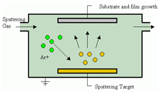
S-Bond soldering is seeing increased application for the solder bonding of sputter targets. Sputter targets are used in a wide range of applications for making thing films used in making electronic chips, solar cells, sensors, TV screens, optical components, electrical devices, and on and on… Sputter targets support a very large physical vapor deposition (PVD) and diverse technological base that is wide ranging and pervasive. Sputter targets under ion bombardment release target material atoms into a high vacuum chamber that under an electric field can be accelerated and deposited onto the component surface where the arriving atoms arrange themselves into a contiguous thin film. Figure 1 schematically illustrates the sputtering process. Ion bombardment is a high energy collisional process that can heat target materials to their melting points unless cooled; hence most sputter targets are bonded to a water cooled backing plate. Backing plates are made normally made from copper and are mounted to a water cooling manifold. Other metallic backing materials are also used. See Figures 2-3 for examples of bonded sputter targets. (more…)
