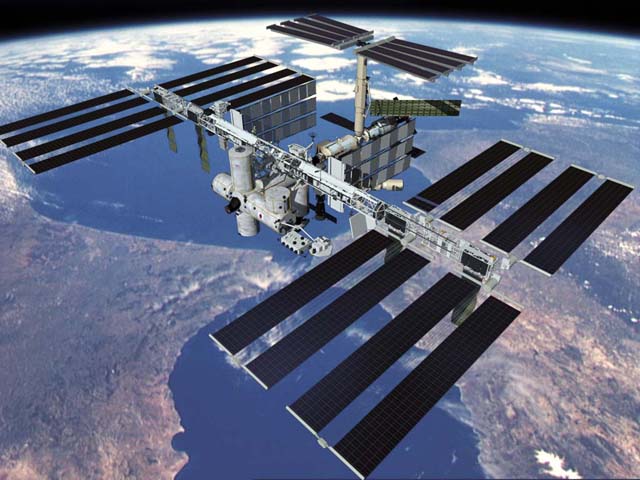
Posts Tagged ‘fluxless solder’

Fluxless Soldering of Sputter Targets

Friday, January 27th, 2012
schematic sputtering process Fluxless Soldering of Sputter Targets

Figure 1. Schematic of sputtering process

S-Bond soldering is seeing increased application for the solder bonding of sputter targets. Sputter targets are used in a wide range of applications for making thing films used in making electronic chips, solar cells, sensors, TV screens, optical components, electrical devices, and on and on… Sputter targets support a very large physical vapor deposition (PVD) and diverse technological base that is wide ranging and pervasive. Sputter targets under ion bombardment release target material atoms into a high vacuum chamber that under an electric field can be accelerated and deposited onto the component surface where the arriving atoms arrange themselves into a contiguous thin film. Figure 1 schematically illustrates the sputtering process. Ion bombardment is a high energy collisional process that can heat target materials to their melting points unless cooled; hence most sputter targets are bonded to a water cooled backing plate. Backing plates are made normally made from copper and are mounted to a water cooling manifold. Other metallic backing materials are also used. See Figures 2-3 for examples of bonded sputter targets.

sputter targets Fluxless Soldering of Sputter Targets

Figure 2. Example Sputter Targets

To manufacture sputter targets, the target materials, such as W, Ti, Cr, Al, Si, InSnO (ITO), Ce, Ga, Au, Pd, Ag, etc. need to be bonded to metallic backing plate. Soldering or diffusion bonding normally are used since a metallic joint is required in order to provide an electrically and thermally conductive structural joint. The soldering process has been a major bonding technique since soldering is simpler and more versatile and can bond a wider range of materials. For ceramic targets such as Indium Tim Oxide (ITO) and other ceramics and intermetallic targets, Indium solders have used. Indium is a mildly “active” metal that can interact with oxide surfaces and can bond a range of metals without extensive use of flux. Most Sn based conventional solders use flux to clean the backing plate surface and/or the plated target materials, but in the wide bond areas required for many sputter targets, flux is trapped in the interface, later causing contamination in high vacuum sputtering systems. Hence, fluxless soldering is desired. S-Bond and indium solders fit this requirement; however, Indium re-melts at 157°C where S-Bond begins to remelt at 220°C. This increased remelt temperature permits higher power inputs translating to higher sputter rates).

S-Bond solder joining is an active, fluxless process where the Ti, Mg, Ce and Ga in the S-Bond solders enable the solder to interact and wet directly to all metals including Cu, Al, Mo, Ti, W, and Si as well as most compounds and ceramics. Since S-Bond joining requires no plating nor does it use flux, the bonding is direct and complete with no flux filled voids.

sputter bond sputter targets Fluxless Soldering of Sputter Targets

Figure 3. Picture of a range of sputter bonded sputter targets

As sputter targets get larger and larger for applications such as 300 mm wafers and TV screens, large differences in coefficients of thermal expansion (CTE) make diffusion bonding impossible as cooling from the bonding temperatures distort and many times crack the targets. Soldering is preferred and the lower the temperature of the joining process the better. For conventional soldering of larger targets, Indium solder is preferred when since the lower melting temperature (157°C) of indium and its mildly active nature creates a bond with less CTE mismatch stresses. However, indium solders to lower the power input ratings and lowers the effective sputtering rates. As such, active Sn-Ag solders such as S-Bond can be used to create stronger bonds and higher temperature (remelts at 233°C) target operation.

In the last few years a new bonding process has emerged which improves the solder bonding of large sputter targets that have large CTE mismatch such as CIGS and ITO used in flat panel displays and in solar panels. The process is NanoBond®. It is a “no temperature” process and in combination with S-Bond as a “tinning layer” to wet the ceramics and refractory metals and in combination with Sn-Ag solder, large targets can be bonded. The NanoBond® process using S-Bond is described more fully in another blog article on this website, but in summary, using patented exothermically reactive foils, the heat generated by the preplaced Nanofoils® into bond interfaces that have been pre-tinned with solder, remelts the solder and bonds the target to the backing plated without bulk heating of the target / backing material.

The NanBond® process is sold through the Indium Corporation and they provide bonding services, materials and license their customers to utilize the NanoBond® process in combination with S-Bond solders to make larger sputter targets of widely mismatched CTE materials.

Contact us for more information on S-Bond solders and how we can improve your sputter target manufacturing processes.

NanoBond®; registered trademark of Indium Corporation.

Ultrasonic Soldering & Active Solders

Monday, October 10th, 2011

S-Bond® active solders are very effective in combination with ultrasonic soldering for a range of applications. Ultrasonic (U/S) soldering is a fuxless soldering process and is finding growing application in soldering of metals and ceramics from solar photovoltaics and medical shape memory alloys to specialized electronic and senor packages. U/S soldering has been reported since 1955 as a method to solder aluminum and other metals without the use of flux. The reason for expanding usage is that ultrasonic soldering is a fluxless process.

U/S soldering uses either ultrasonically coupled (piezoelectric ) heated solder iron tips (0.5 – 10 mm) or solder baths. These devices generate high frequency (20 – 60 kHz) acoustic waves to mechanically disrupt oxides that form on the molten solder surfaces and/or initiates cavitation in the solder pool which also mechanically disrupt oxide layers that naturally formed on metal surfaces being joined. Cavitation in the molten solder pool can be very effective in disrupting the oxide on many metals, however, it is not effective when soldering to ceramics and glass since they themselves are oxides or other non-metal compound that cannot be disrupted since they are the base materials. A schematic of the U/S soldering process is illustrated below.

ultrasonic soldering Ultrasonic Soldering & Active Solders

U/S soldering consists of heated soldering tips coupled to a piezoelectric crystal that is powered by an acoustic amplifier operating at 20 – 60 KHz. The tips for U/S soldering irons are also coupled to a heating element while the piezoelectric crystal is thermally isolated, not to degrade the piezoelectric element. The tip thus can heat (up to 450°C) and mechanically oscillate at 20 – 60 KHz. This soldering tip can melt solder filler metals as acoustic vibrations are induced in the molten solder pool. The vibration and cavitation in the molten solder then permits solders to wet and adhere to many metal surfaces. Initially, U/S soldering aimed at joining aluminum and other metals; however, with the emergence of active solders, much wider range of materials can be soldered c using ultrasonics as a form of mechanical activation.

U/S soldering is now expanding in application, since fluxless active solders are increasingly being requested for joining assemblies where either corrosive flux can be trapped or otherwise disrupt operation or contaminate clean production environments or there are dissimilar materials / metals / ceramic/ glasses being joined. In this expanded list of materials, active solders’ own nascent oxide on melting need to be disrupted and U/S agitation is well suited.

ultrasonic soldering dissimilar materials Ultrasonic Soldering & Active Solders

Active solders such as S-Bond and other activated solders that use rare earth elements, Ti, Hf, Zr or even indium all form a tenacious oxide on their molten surfaces and conventional solder fluxes to not disrupt these. In applications where the area of the solder joint is a small or band, U/S soldering using 1 – 10 mm tips can be very effective since the volume of molten metal is small and can effectively be agitated by the 1 – 10 mm U/S soldering iron tips. The figures in this article show the U/S soldering equipment (power supply and soldering tools-tips) and the application of solder to glass using U/S solder iron tips. In other larger surface bonding application, as shown in the image below, wide, heated U/S tips are being used to spread and wet active solders on large aluminum surfaces (and is applicable to other metal, ceramic and glass surfaces.

ultrasonic soldering surface bonding Ultrasonic Soldering & Active Solders

One can see that with the commercial introduction of active solders, such as S-Bond®, U/S soldering has expanded well past it use to aluminum and is finding wider and wider application. S-Bond Technologies maintains a U/S soldering development laboratory and offers both development and production services. Contact Us to evaluate if U/S soldering can be beneficial and applicable in your applications.

S-Bond Develops Fluxless “Hybrid” Soldering Techniques

Tuesday, May 18th, 2010

Hybrid S-Bond joining processes eliminate the use of fluxes and have been shown to be more effective since it completely joins with the S-Bond filler metals. The methods that are recommended to minimize the use of S-Bond, yet still achieve fluxless joining are as follows:

  • Heat base materials to S-Bond melting temperature.
  • Melt a small amount of S-Bond onto the joining surfaces.
  • Add ~ 0.1g/cm2 to the opposing surfaces to be joined
  • Add S-Bond to the opposing joint surface.
  • Mechanically spread the S-Bond layer to completely cover the joint area (brush, spatula or ultrasonics).
  • Melt “conventional” solders onto the S-Bond layer on the bottom base and agitate to assure wetting to the underlying S-Bond layer.
    NOTE: Sn-Ag, Pb-Sn, Sn-Bi, In solders can be used
  • Add enough “conventional” solder to the base to “float” and slide the top surface of the joint onto the conventional solder and provide excess solder to fill any gaps.NOTE: The sliding of the molten S-Bond / solder surfaces onto one another eliminates entrapped air and mechanically shears the surfaces of the S-Bond layer to the bottom “conventional “ solder layer on the base.

S-Bond to Sell EWI’s Lead-free, Fluxless Solder

Tuesday, May 18th, 2010

S-Bond Technologies and EWI have signed an agreement granting S-Bond Technologies the ability to distribute EWI’s patented lead-free, fluxless solder marketed by EWI as EWI SonicSolder®. The agreement is effective immediately. SonicSolder® is an active solder that permits the cost effective fluxless joining of aluminum, copper, other metals, glass, and ceramics without the need for plating.

Dr. Ronald Smith, President of S-Bond Technologies stated, “We are pleased to partner with EWI in growing the application of active, fluxless solder joining technologies. We see our partnership with EWI and our licensing of its SonicSolder® technology as an enhancement to our own patented active solder product line, S-Bond® and broadens our capabilities to provide more cost effective assembly solutions.”  Henry Cialone, President and CEO of EWI said, “We’re excited to partner with S-Bond Technologies, further leveraging our patent in the marketplace. The partnership gives S-Bond a nice addition to its already strong portfolio of solder that will hopefully open up new markets for them with its cost-effective pricing.”

About EWI SonicSolder®
EWI SonicSolder® is an EWI patented binary lead-free solder alloy that melts at 231°C. In conjunction with ultrasonic soldering, it can be used to join difficult-to-wet materials like aluminum, titanium, glass, and ceramics and dissimilar materials. Potential applications include tubing, electronics, medical products, and structural components. In various metal-metal (copper, aluminum, titanium) combinations, shear
strength of about 5 ksi has been obtained. The solder will be available in a variety of forms in early 2010 but currently ingot materials can be purchased. For more information, visit www.s-bond.com

About EWI

EWI is a leading engineering and technology organization dedicated to materials joining and allied technologies. We provide applied research, manufacturing support, and strategic services to nearly 2,800 member company locations of global leaders in the aerospace, automotive, defense, energy and chemical, government, heavy manufacturing, and electronics industries. Visit ewi.org for more information.