S-Bond Joining of SiC Tiles in Microwave Beam Dampers (Absorbers)
Argonne National Laboratories selected S-Bond active solder technology to make water cooled high power microwave beam dump in its Advanced Photon Source which is a user-facility to producing extremely brilliant x-ray photon beams. The Advanced Photon Source uses high energy microwave beams to steer and create such x-ray photon beams. These beams once started cannot be shut down or restarted easily, so to facilitate the use the various beam lines, the microwave beams are diverted to beam dumps. These beam dumps consist of microwave cavities that are lined with SiC tiles bonded to water cooled rectangular copper enclosures that are heavy water cooled. SiC is a well know high efficiency absorber of microwave energy and thus is used in dampers.
The challenge faced by the Argonne engineers and physicists was to find a stable process for bonding the SiC tiles to copper bases that would provide thermal and electrically conductive interface and be able to take the thermal expansion mismatch during the bonding processes and in service. Active brazing and active soldering were considered since active brazes and solders are able to form metallurgical bonds with the SiC tiles. Active brazing, using Cu-Ag-Ti was tested and it was found the residual stresses stemming from the coefficient of thermal expansion (CTE) mismatch of SiC and copper led to the fracture of the SiC tiles upon cooling from the 860˚C brazing temperature to room temperature. S-Bond active soldering was selected as good alternative to active brazing since the solder bonding temperature of 250˚C yielded much lower CTE derived stresses and created a more compliant bond line that would better accommodate the heating and cooling stresses in service.
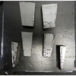
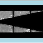
Figure 1 below show the S-Bond joined SiC tiles being bonded into one half of the microwave beam damper cavity indicating how S-Bond successfully joins SiC to copper. Figure 2 is an ultrasonic C-Scan of the bonded interfaces under each tile in the damper half
Contact us to see how S-Bond joining can solve your ceramic to metal bonding challenges.

