215.631.7111

S-BOND BLOG

Active Solder Joining for Semiconductor Processing

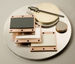
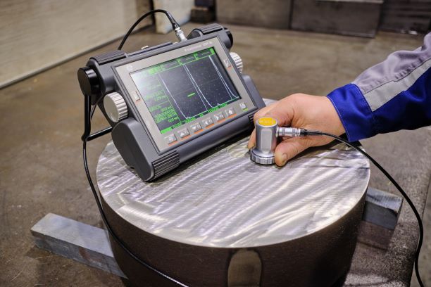
S-Bond Technologies’ active solders are finding wide application in semiconductor processing equipment. Their capability to join a wide range of dissimilar materials and the fact that as a filler metal, their bonds are thermally conductive make S-Bond solders far superior to many other commercial bonding/thermal interface materials. Semiconductor processing applications include…

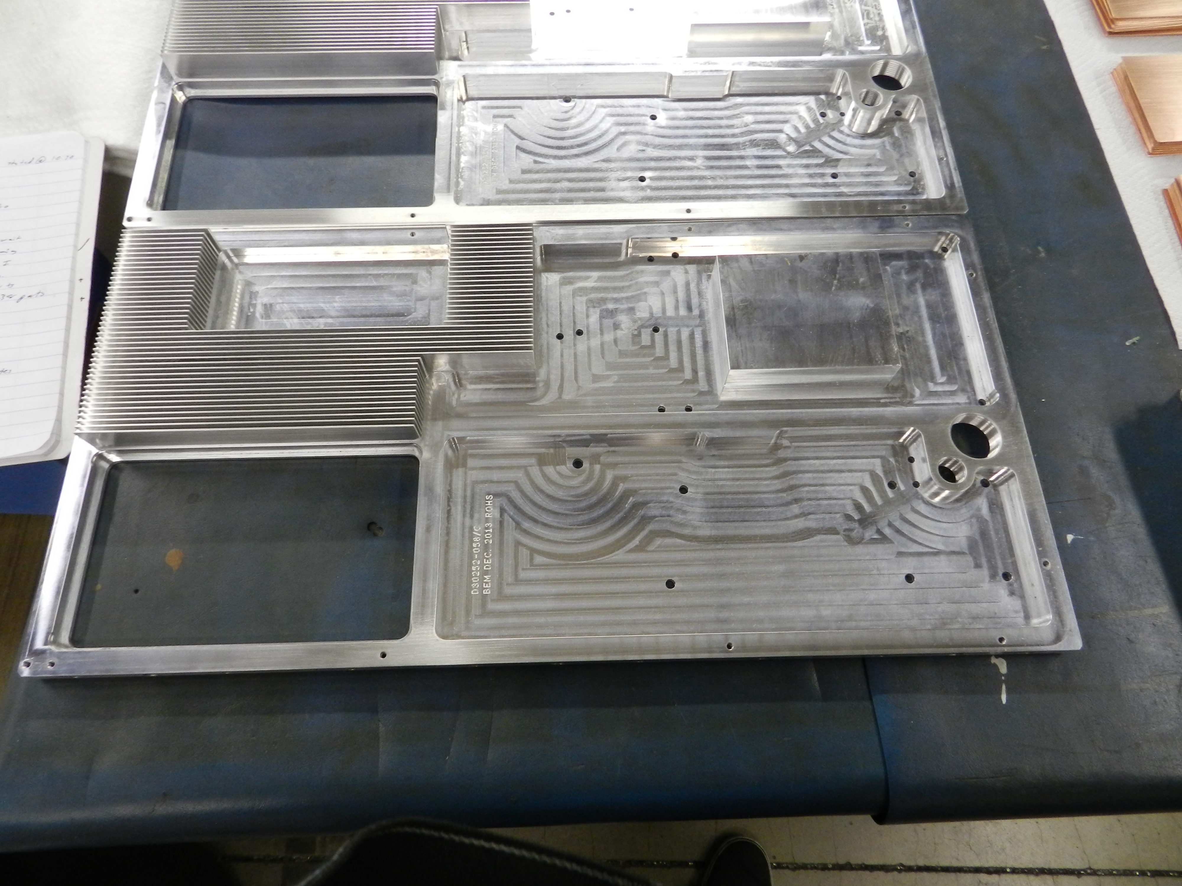
In sputter targets, the deposition/target materials is sputtered (high energy ion impacts displace a target’s atoms) onto an opposite surface to form a functional coating or other element layer in a computer chip, TV screen or other semiconductor device. The high energy impact of the deposited films require “sputter targets” to be cooled to keep the target material layer from melting. To cool the target, water is circulated in an aluminum or copper base plate.  S-Bond active solders can bond all metals and most ceramics that are commercially used to produce sputtered films. Active solders can bond these sputter targets to either Copper or Aluminum, bonding them at low temperatures (which minimizes thermal expansion mismatch stresses), without flux contamination/entrapment (which will contaminate the sputtering plasma), and with excellent thermal conductivity (a metallic bond with nearly no voids).

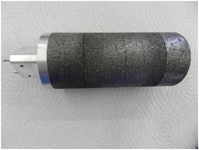
For probes and sensors, S-Bond active solders can bond silicon or carbide/carbon based devices (MEMS or other semiconductor based probes) directly to metal and metallic conductor leads. The low temperature active solders, when joining semi-conductor devices, impart low residual stresses and the joints are electrically and thermally conductive… good for signal transmittance and cooling.

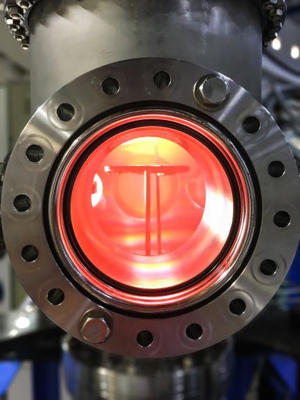
Piezoceramics such as Pb-Zirconates (PZT) that impart force/small displacement or create ultrasonic pulses, can be bonded direct to metals with active solders. Bonding is accomplished bonded below their curie points with acoustically sound interfaces that can transmit sound effectively.  Such piezoceramic based sensors and actuators are used in accurately measuring gas flow and can be used on gas control in MOCVD processes used to deposit and etch computer chips. S-Bond active solders can wet and adhere to most piezoceramics all without pre-plating and chemical fluxes… as such they are finding excellent application in probes and sensors used on semiconductor processing.

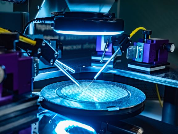
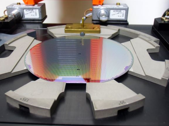
Wafers (silicon or other) are placed into energetic plasmas and other beams to deposit then etch a complicated surface morphology in layers to create semiconductor based chips. The high heat energy into the wafer needs to be removed through water cooled wafer handling devices such as the pedestals the wafer sits on in their processing chambers. If not cooled, the interdiffusion of the fabricated on the wafer. With the latest 300mm diameter wafer technology over a $1M work of chips can be on a wafer.

The high energy levels used in semiconductor processing requires well cooled and reliable handling equipment. S-Bond active solders can intimately join copper and aluminum as well as other thermal management materials such as AlSiC and pyrolytic graphite

If you would like to see how S-Bond active solders can improve your semiconductor processes and handling and measuring equipment, please Contact US.

Sensors and Actuators

Sensors and actuators are a growing commercial market with the Internet of Things (IOT) and the interest to remotely monitor and control many devices.

S-Bond® active solders are finding more application in sensors and actuator devices due to their use of dissimilar materials, including metals, intermetallics, ceramics, composites and glasses which need to be joined. S-Bond® active solders are unique in that they can join such materials, without flux or plating, at low temperatures and with excellent conductivity (both electrical and thermal).

S-Bond® active solders can bond…

  • All metals (Al, Cu, St. Steel, Ti, W, Mo, Ni, etc)
  • Ceramics (Al2O3, SiO2, Sapphire, Quartz, Zirconia, AlN, Si3N4, etc)
  • Carbon / Carbides (SiC, TiC, WC, Graphite, Diamond, etc)

With Ce, Ga and Ti additions to solder filler metals, S-Bond® solders can bond direct to oxides, nitrides and carbides that have formed on metal surfaces, directly. On aluminum and copper the Ga and Ce interact with the oxides that form on these metals then the Sn and Ag constituents form metallurgical intermetallic compounds (IMC’s) that chemically bind the solder to the aluminum or copper base metal. With the active S-Bond® solders’ ability to wet, adhere and join such a diverse set of materials, the S-Bond® alloys find wide application in sensors and actuators that employ a diverse array of materials and in dissimilar material joints… These joints have many requirements, depending on the application, these requirements include…

  1. Thermally conductive
  2. Electrically conductive
  3. Transmits sound
  4. Hermetically seals
  5. Bond strengths high enough for the application
  6. Low temperature joining
  7. Accommodation of CTE mismatch strain

Sensors and Actuators that S-Bond® is currently specified in includes…

Piezo ceramic (PZT) – Ultrasonic Gas Flow sensors; PZT ceramic disks are S-Bond® soldered to stainless steel housings that transmit and receive u/s sound pressure waves. The transmit sensor with bonded PZT piezo ceramic disk sends u/s waves into a passing gas flow and a receive sensor with bonded PZT receives and converts the sound waves… with a shift in frequency known as the Doppler effect, can relate the frequency shift to the mass flow of the passing gas stream. In these sensors, the piezo ceramic disk needs to be intimately bonded with no voids to create an acoustically “hard” transmitting bond interface, joining the ceramic to metal below the curie temperatures of 250 C.  S-Bond® 220 alloys are being used to make these reliable and acoustically sound interfaces.

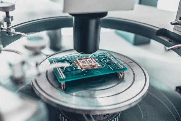
MEMS Pressure Gages; Silicon based MEMS devices us Si-dies and incorporate circuitry to use the Si as part of the measurement. In the case of pressure measurements, thin diaphragms of Si are created and strain gage circuitry is deposited using lithography to complete the sensor… the challenge then was so seal the Si-sensor die to a metallic pressure housing that is installed onto the component needing a pressure sensor. S-Bond® active solders can join Si direct to metals and can create a hermetic joint, creating a seal between the Si-MEMS pressure sensor and the mounting housing.

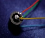
Graphite Electrodes / Water Conductivity Sensors; S-Bond® active solders are being used to join graphite to electrical leads for use in Anode/Cathode systems for making excellent electrical solder connections with the use of flux or pre-plating.


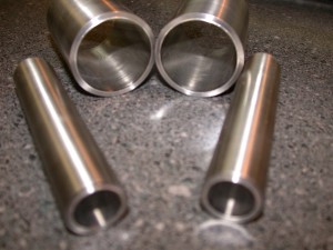
Sapphire – Optical Sensors; Sapphire is single crystal aluminum oxide that is very hard/scratch resistant and also transits optical signals in a specific spectrum. As sapphire is an excellent “window” material for many optical signals. For example in Gamma Ray Detection, NaCl single crystal creates photon (light) output proportional to the impinging gamma ray radiation intensity.  The NaCl crystal will degrade/dissolve in contact with air, to the crystal is housed behind a sapphire window which is S-Bond® active solder sealed (hermetic/He leak free) to a titanium tube to create a sealed environment that the gamma rays can penetrate. Optical detectors are then mounted in front of the sapphire window, outside the S-Bond® sealed enclosure.

Insulators /Radar Sensors; Printed 3-D circuits are being made to generate / receive radar signals.  These circuits are built through ceramic layers that form a ceramic backbone to the sensors’ circuitry. S-Bond® active solders have been used to bond the edges of this ceramic backbone of the sensor and seals it from the environment.

Magnet Assemby – Actuators; Magnetic actuators are used to move valves, switches and other devices dependent on precise and reliable stroke based motion. Such magnetic actuators are using high force as CoSm based magnets. These magnets will form a strong and specific magnet fields. In one actuator design, the actuator “rod” runs on the magnet assemblies’ magnetic axis. To assure optimal actuator lineal translation, the actuator’s central push rod could not be magnetic, so it a ceramic rod was selected. In this actuator, S-Bond® active solders have been used to bond the central ceramic rod to the magnetic core of the actuator.

As presented here, S-Bond® solders are being applied in a growing range of sensors and actuators. If you would like to take advantage of S-Bond® solders unique capabilities to join dissimilar materials in your sensors and actuators, please Contact Us.

Rotating Graphite:Metal Seals

2014-06-20 036
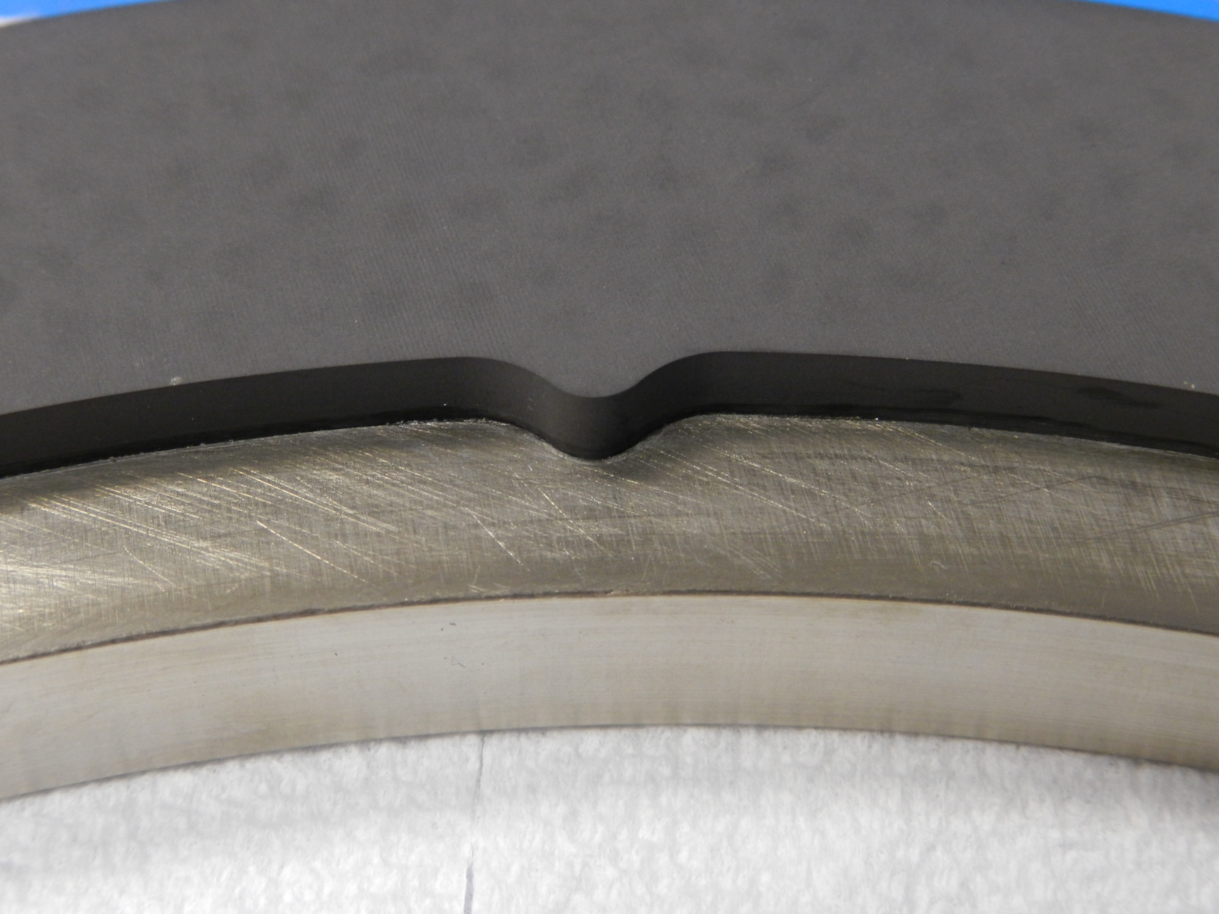
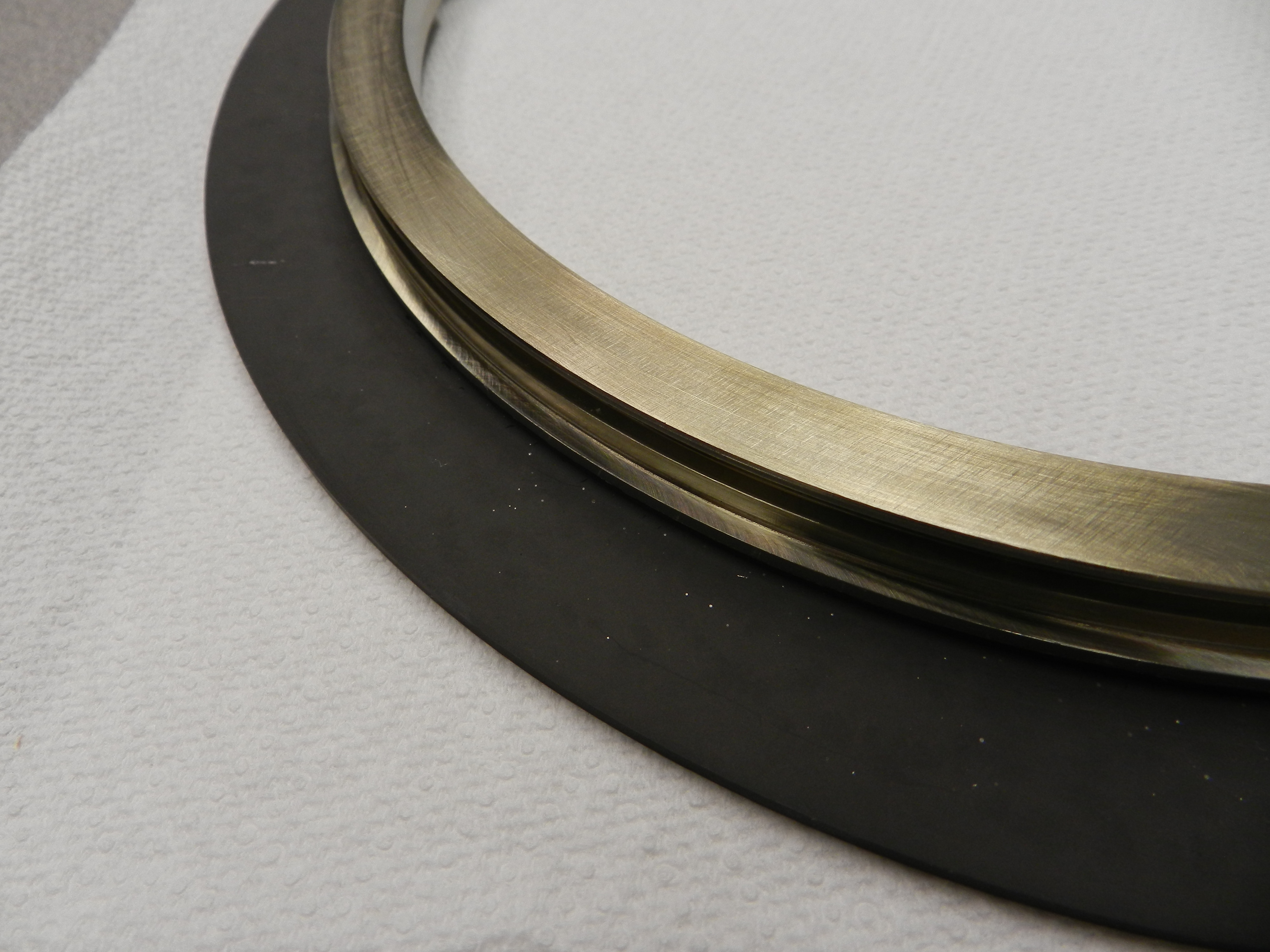
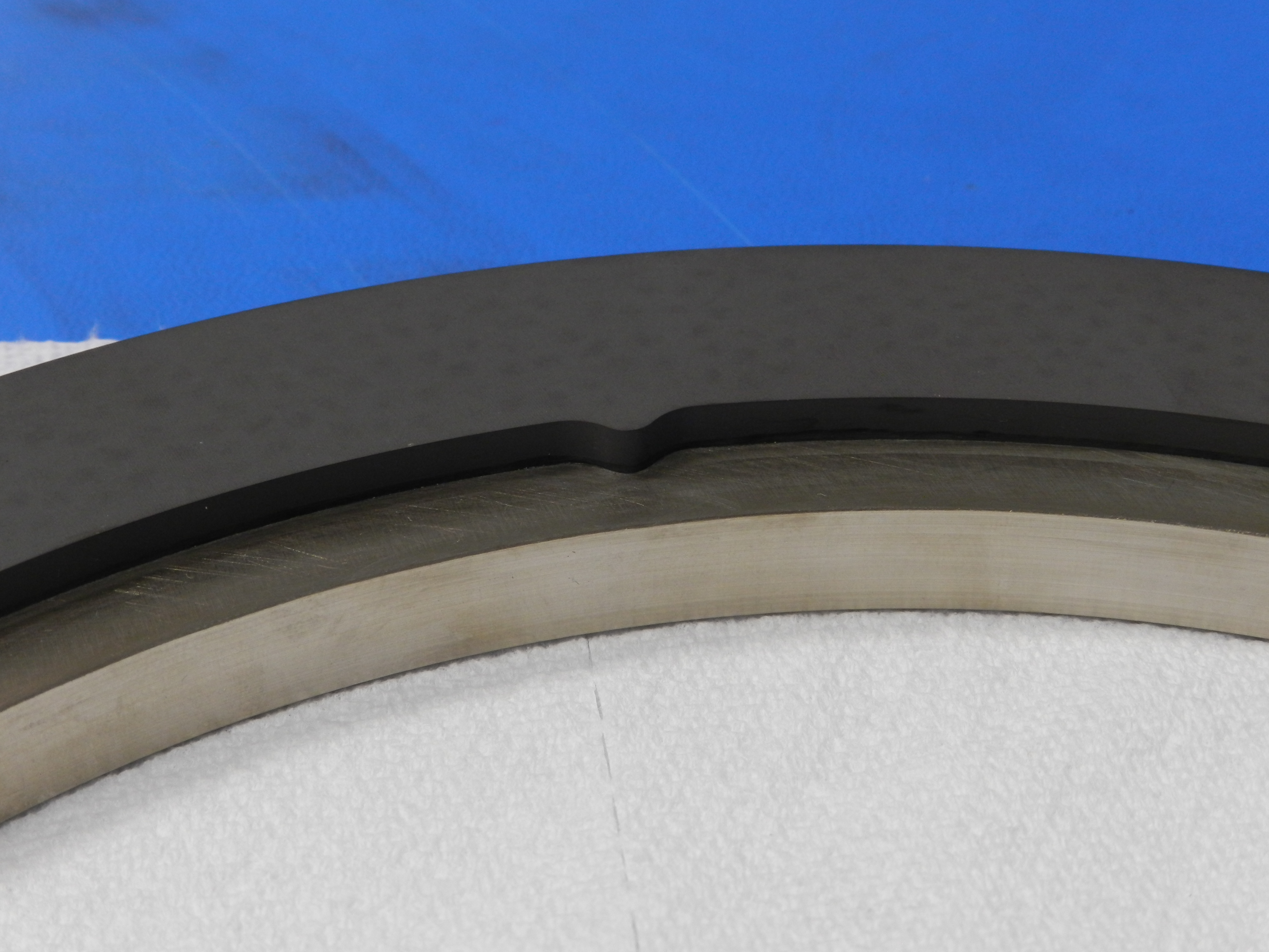
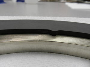
Carbon/graphite compressor seal rings are employed in many compressors and more and more metal backed graphite seals are being used in higher efficiency compressors. Frictional heating of seals can degrade metal backed graphite seals, therefore good thermal contact between the graphite seal ring and the metal backing is needed to improve cooling of the seal. S-Bond Technologies has developed active soldering methods for graphite bonding which is now being used to manufacture rotating metal backed graphite seals.

In the process, graphite rings are initially S-Bond metallized to create a chemically bonded solder to graphite interface. The sequence of bonding is shown in the figures below. After metallization the metal rings’ bonding surface are pre-tinned with S-Bond filler metals, via heating, melting of the solder surfaces on the metal followed by mechanical activation (ultrasonic solder tip agitation). The metallized graphite ring surface, at 250C is pressed against the pre-tinned metal backing ring surface and then the assembled ring is cooled to solidify the solder joint.

These S-Bond solder joined graphite to metal backing ring seals have endured 1,000’s of hours of running in natural gas compressors and are providing the customer with improved graphite – metal backed ring seal performance.

Please Contact Us for your graphite to metal bonding solutions.

2014-06-16 138
2014-06-16 222

2014-06-16 224

2014-06-20 063
2014-06-20 040

Fabrication of Hybrid Cu-Al Finned Heat Sinks

DSCN7334
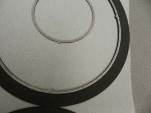
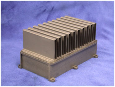
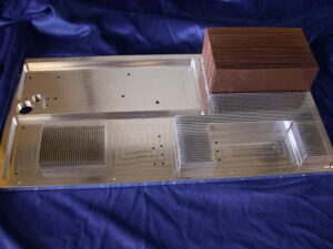
Copper has superior cooling capacity than aluminum and is the preferred heat sink material for telecommunications and high power electronics. However, the weight and cost or copper limits the size of the heat sink packages. Therefore for larger electronic enclosures a hybrid design, using copper for a localized heat sink joined to an aluminum frame with good thermal contact can significantly improve the cooling performance of a heat sink package.

Joining copper to aluminum poses it challenges. Cu and Al cannot be welded easily due to the intermetallics that form when Cu alloys with Al in the weld pool. Alternatively, brazing cannot be done since melt point of aluminum is below the typical Cu-Ag braze filler metals (silver solders) used to braze copper. These issues leave “soldering” as the metal filler joining process of choice. But alone, soldering of Cu to Al has challenges. Solders, typically Sn-Ag based, cannot easily wet and adhere to aluminum without first plating the aluminum with nickel or using very aggressive chemical fluxes which themselves are incompatible with soldering to copper.

S-Bond Technologies, working with its customers has demonstrated its active solder, S-Bond 220-50, join Cu to Al in all configurations. The figures below show an example of where a copper- finned heat sink assembly was S-Bond joined into a finned aluminum package. In this assembly, the Cu-fins were individually S-Bond soldered into copper heat sink base, after which the Cu fin-base assembly was then S-Bond joined into the aluminum base at 250C. This soldering temperature well below the softening temperatures for the aluminum frame and low enough that the thermal expansion mismatch between Cu and Al did not distort the bonded assembly when cooling.

Hybrid heat sinks, combing the thermal benefits of copper with lightweight aluminum are taking advantage of the capabilities of active solder joining. For tough dissimilar materials and copper and aluminum bonding challenges, Contact us.

2014-01-07 1222014-01-07 110 2014-01-07 114

Carbon:Carbon Joining for Fermi Lab’s Particle Physics Detectors

2013-03-25 054S-Bond Technologies’ active solder joining solutions have been used by by Fermi National Accelerator Laboratory for joining carbon:carbon and pyrolytic graphite in its particle accelerator program.  The improved Forward Particle Detector (FPIX) is to be used in Compact Muon Solenoid (CMS) and used for high-resolution, 3D tracking points, essential for pattern recognition and precise vertexing, all embedded in a hostile radiation environment.

The challenge posed by Fermi Lab to S-Bond Technologies, was to create high thermal conductivity metallic bonds between the ends of thermally pyrolytic graphite (TPG) blades and carbon:carbon composite end walls of a turbine nozzle like assembly. Figure 1(a-b) shows ¼ of a full assembly that was built using S-Bond joining and S-Bond 220 solder and processing. S-Bond’s active solder processing was successfully demonstrated and is in the technical roadmap for assembling Fermi Lab’s particle accelerator FPIX.  In this work, regular adhesives were not conductive and would off-gas in the extremely high vacuum environments, hence the selection of the active metal solder filler, S-Bond 220.

2013-03-25 058


Figures 2 – 4 show various assembly steps that all utilize the S-Bond carbon:carbon joining process described elsewhere in our technical blog. The process started with the S-Bond metallization on the TPG blades, Figure 2,  and the C:C nozzle endwall slots

2013-02-26 407
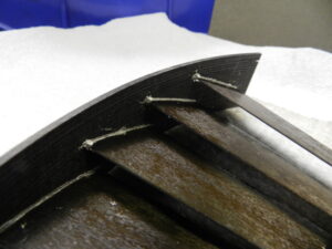
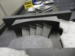
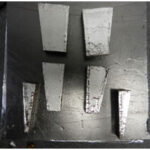
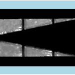
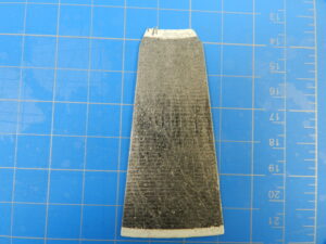
where the blades were inserted, Figure 3. After metallization, the blade and nozzle segments were inserted into a heated alignment press, Figure 4. After heating and insertion, the nozzle segment/ TPG blade assembly was cooled and removed. Figures 1a – b, above, showed the final fully bonded assembly.
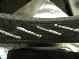


2013-03-25 007

Assy-FermiNozzle1


Please contact us if you have challenging graphite / carbon joining applications where S-Bond Technologies active solders can solve your joining problems.

S-Bond Joining of SiC Tiles in Microwave Beam Dampers (Absorbers)

Argonne National Laboratories selected S-Bond active solder technology to make water cooled high power microwave beam dump in its Advanced Photon Source which is a user-facility to producing extremely brilliant x-ray photon beams. The Advanced Photon Source uses high energy microwave beams to steer and create such x-ray photon beams. These beams once started cannot be shut down or restarted easily, so to facilitate the use the various beam lines, the microwave beams are diverted to beam dumps. These beam dumps consist of microwave cavities that are lined with SiC tiles bonded to water cooled rectangular copper enclosures that are heavy water cooled. SiC is a well know high efficiency absorber of microwave energy and thus is used in dampers.

The challenge faced by the Argonne engineers and physicists was to find a stable process for bonding the SiC tiles to copper bases that would provide thermal and electrically conductive interface and be able to take the thermal expansion mismatch during the bonding processes and in service. Active brazing and active soldering were considered since active brazes and solders are able to form metallurgical bonds with the SiC tiles. Active brazing, using Cu-Ag-Ti was tested and it was found the residual stresses stemming from the coefficient of thermal expansion (CTE) mismatch of SiC and copper led to the fracture of the SiC tiles upon cooling from the 860˚C brazing temperature to room temperature. S-Bond active soldering was selected as good alternative to active brazing since the solder bonding temperature of 250˚C yielded much lower CTE derived stresses and created a more compliant bond line that would better accommodate the heating and cooling stresses in service.

Figure 1 below show the S-Bond joined SiC tiles being bonded into one half of the microwave beam damper cavity indicating how S-Bond successfully joins SiC to copper. Figure 2 is an ultrasonic C-Scan of the bonded interfaces under each tile in the damper half

Contact us to see how S-Bond joining can solve your ceramic to metal bonding challenges.

S-Bond Joined Phase Change Materials (PCM’s) Heat Sinks

S-Bond® active solders are being used extensively as a high conductivity bonding solution for foam cored phase change materials foam cored heat sinks. Increasingly, thermal management in electronics is the limiting factor in performance and/or life of electronics as higher power and higher speed in electronic devices generate more intense heat. High brightness LED’s, high speed/high bandwidth telecommunications, avionics, satellites and solid state conversion devices all have transient and steady power states where intense heat is generated and needs to be channeled away from the electronic device to prevent performance loss or permanent damage. The electronic industry is relying on a host of devices from conventional heat sinks with fins and fans to heat pipes and vapor chambers to more exotic materials and composites that include pyrolytic graphite or diamond. S-Bond materials and processes have been proven to be a good solution when bonding these various components and materials with a metallic “thermal interface material (TIM)” rather than filled polymeric bonding agents.

When electronics have a high transient heat output thermal engineers are using “phase change” heat sinks. Such heat sinks utilize “phase change materials (PCM’s)” that when exposed to heat absorb it very quickly and effectively as the material “changes phase”… either going from solid to liquid or liquid to vapor. Materials with high latent heats of fusion or latent heat of vaporization at or near the maximum temperatures that electronics are being used in the core of such heat sinks. In PCM heat sinks during the phase change there is the potential to rapidly absorb a high heat load… that can later be more slowly released to the atmosphere with cooling fins as the phase change is reversed and the heat is released away from the electronic device.

Two of the most used PCM’s are paraffin and water… each has a high latent heat of fusion or heat of vaporization, respectively. The challenge in the use of PCM’s is to overcome their relatively low thermal conductivities. For example, in heat sinks with paraffin as the PCM, when the heat transfers from the electronic device into the heat sink package, the outer layer of paraffin melts and then slows the transfer of heat into the solid paraffin core. To offset this heat flow limitation, designers are incorporating metallic or graphitic foams into the core of the heat sinks. The foams’ cells separate the PCM’s into small reservoirs that are surrounded by high thermal conductivity cell walls that then transfer the heat to a small PCM filled pore in the foam and therefore quickly melts the paraffin or vaporizes the water. Later in the “reverse” cycle, the conductive foam “cell walls” transfer the heat out of the PCM filled pores to solidify or condense the full volume PCM in the heat sink.

S-Bond joining has found excellent application in paraffin based PCM heat sinks in combination with graphitic foams (PocoFoam® or K-Foam®). S-Bond can effectively bond to graphite and graphite foams to heat sink package materials such as aluminum, copper and many heat sinks composites such Al-SiC, Al-Gr, Cu-W or Cu-Gr. In such graphite core/paraffin heat sinks. S-Bond Technologies has S-Bond metallized the Gr-Foam preparing for it to be soldered directly to the heat sink package. After S-Bond metallization, various S-Bond solders and processing can be used to bond the graphite foam to the components of the heat sink.

Heat Sink for Laser Diode Packages
Figure 1. Paraffin “PCM” / Graphite Foam cored heat sink for laser diode packages.

Figure 1 shows a PCM core finned Aluminum heat sink box used to cool high power laser diode packages mounted on the flat side opposite the side with the fins. The aluminum box contains a core of graphite foam bonded to the walls and base of the aluminum enclosure. The aluminum enclosure is then heated to 100˚C and filled and infiltrated with paraffin PCM’s. After filling the enclosure is sealed and the assembly is a PCM heat sink. When the laser diodes are on for intermittent periods of time the graphite foams thermally bonded to the wall of the enclosure heat the PCM… later when the heat load from the diodes are off, the bonded fins with air convection assist, cool and solidify the paraffin PCM to get the heat sink ready for the next thermal cycle. S-Bond active solder joining enabled the graphite foam to have an excellent thermal interface to the enclosure without filling the graphite foam and compromising the graphite foam’s ability to hold and transfer heat quickly to the paraffin PCM.

Heat Sink for Hot Fluid Channeled into Core
Figure 2. Graphite foam cored PCM heat sink for hot fluid channeled into the core.

Figure 2 shows another type of PCM cooling. The alternating bonded fluid circulating aluminum tubes bonded with S-Bond sandwiched between S-Bond metallized and bonded graphite foam plates. The stack is later encased in an enclosure and paraffin PCM is infiltrated into the foam to make a large ~ 24” x 24” x 12” PCM heat sink. When heated fluids circulate in the aluminum tubes the PCM filled graphite foam core rapidly absorbs the heat from the fluid.

Graphite foam wrapped heat pipe PCM heat sink
Figure 3. Graphite foam “wrapped” heat pipe PCM heat sink.

Figure 3 illustrates another style of PCM heat sinks that are mounted around a central heat pipe. In this design, S-Bond metallization of the faces and ID’s of the graphite annular rings permitted a graphite foam outer core to be become an effective PCM heat sink for a heat pipe cored thermal management device.

Contact us to evaluate how S-Bond can be used to enable your thermal management components to be made and how phase change material (PCM) heat sinks can be effectively incorporated into your designs.

New Lower Temperature Active Solders Developed

S-Bond Technologies has developed and proven a new, lower temperature active solder that melts from 135 – 140°C. The solder, S-Bond® 140 is based around the Bismuth-Tin (Bi-Sn) eutectic composition. This new solder is a lower temperature active solder that enables multi-step soldering where previously soldered connections/seals are not remelted. Active solders that melt below 150C are also finding use in thermally sensitive applications where Sn-Ag based solders that melt over 215°C can thermally degrade the component parts being assembled. Lower temperature soldering also can more effectively bond dissimilar materials where thermal expansion mismatch many times fractures or distorts an assembly’s component parts.

S-Bond 140 is already finding application in glass-metal seals in electronic packages where higher temperature soldering alloys would have damaged the packages’ components. S-Bond 140 is also being used to bond heat pipes and vapor chamber thermal management devices to protect the thermally sensitive phase change fluids from damaging the devices when solder bonding to electronic and LED devices.

Electro-optical package to be bonded to heat sink with S-Bond® 140

Joining of Heat Pipes and Vapor Chambers

Figure 1. Illustration of vapor chamber heat spreader with CPU heat source

Heat pipes and vapor chambers are used to transfer and/or spread heat from concentrated heat sources such as high brightness light emitting diodes (LEDs) and high computing speed CPUs. These active thermal management devices are enclosures/tubes that have porous wick materials lining the walls that provide condensation surfaces and small connected pores that via capillary force, transfer condensed fluids that were originally vaporized at heat source surfaces. When the vapor is transported via convection to the cooler surface to condense, the fluid is then channeled back to the heat source surfaces in a continuous cycle, in effect pumping the heat out of the package without using external power surfaces. Figure 1 illustrates a vapor chamber used to cool a mounted CPU.

Figure 2. Light emitting diode package bonded to vapor chamber

Thermal management is critical in the life and performance of such electronic components that all employ a variety of thermal interface materials (TIMs). With increased power and speed, the polymer-based TIMs being used today are limiting and metal bonding with solders is growing in application. Conventional Sn-Ag soldering temperatures can overheat the thermal fluids in heat pipes and chambers while Indium (In) solders are expensive and do not bond as well as active solders. Responding to this need, engineers at S-Bond® Technologies have announced its latest alloy, S-Bond® 140 as an effective TIM for bonding CPUs or LEDS to heat pipes and vapor chambers.  The Bi-Sn-Ag-Ti alloy can wet and join to all metals including aluminum and to most ceramics and glasses.  S-Bond® 140 is lead free, does not require plating and flux thus keeping electronic and LED packages clean.

Figure 3. S-Bond 140 bonded heat pipe assembly

Figure 2 illustrates a high brightness LED array that has been bonded to a Ni-plated copper vapor chamber with S-Bond 140 solder. This technique provides a high strength and high thermal conductivity metallic solder bond. Figure 3 is another example showing S-Bond 140 solder bonding copper heat pipe tubes (water as the phase change fluid) into aluminum slots to enhance the cooling from the heat pipe to the aluminum package base without plating and flux.. Normally when soldering heat pipes over 200°C, the water in the heat pipe goes to vapor and the resultant pressure distends/distorts the thin copper tube walls. Lower temperature metallic solders, such as S-Bond 140.

Contact us for more information and to order our S-Bond products.

Design Considerations for Solder Bonding

Solder bonding is a versatile lower temperature bonding process that is used in joining a range of metals, ceramics, glass and metal: ceramic composites. By definition, solders are joining filler metals that melt below 450°C. Solder bonding is typically used in the assembly of structures for its good thermal and/or electrical contact or for creating seals. The advantage of solder bonding stems from lower temperature exposure (less that 400°C), compared to brazing when joining thermally sensitive materials.  Alternatively, compared to bonding with epoxy adhesives, solder bonding is a more conductive bond, but does require higher temperature exposure and the wetting of the molten metal to the bonding surfaces.

Figure 1. S-Bond joined heat pipe assembly bonding copper pipes to aluminum base

Because of it excellent thermal and electrical conductivity, solder bonding finds application in the manufacture of sputter targets, heat spreaders and cold plates and other related thermal management components. Solder bonding is also used to seal ceramic:metal and glass windows used in optical based sensors and in other fluid cooled enclosures.  Figures 1 and 2 show several typical solder bonded parts.

Solder bonding (e.g. S-Bond®), despite being versatile and capable of joining most materials, one must consider several issues when active solder bonding…

  • Thermal expansion mismatch
  • Size and shape of bonded parts
  • Interaction with post solder bond processing
  • Galvanic corrosion coupling
Figure 2. Aluminum to copper cooling tubes and ceramic to plated copper sputter targets.

In every application being evaluated for a solder bonding solution, the component and process design needs to consider the following issues.

  • Minimize CTE mismatch of bonded materials to prevent distortion or fracture.
  • Understand post bonding processes to prevent damage of bond interface.
  • Know Service Temperature and Thermal cycling effects on bond interface.
  • Understand effects of service environment on bond interface corrosion

Thermal expansion mismatch (CTE): solder bonding requires heating the component parts in an assembly to 120 – 400°C, depending on the solder filler metal being used.  When similar materials are being joined there is no CTE mismatch so it is not a concern. However; many times solder bonding is being used to lower the CTE mismatch… but despite the lower bonding temperature, it is not alone a “silver bullet” universal solution. Even when heating to 250°C, melting for Sn-Ag based solders, upon cooling once the solder solidifies it can transfer a strain. Then the CTE derived stresses can distort metal assemblies, fracture a glass or ceramic components or fracture the bond. Thus, one needs to minimize CTE mismatch stresses by selecting assemble component materials that are as close as possible in CTE.

When matching CTE is not practical, then one should design the component parts with size and thickness in mind… larger bond areas will “accumulate” more stress and lead to more distortion and/or fracture. A solution for larger parts is to “tile” the component parts; by tiling (mosaic) the strain mismatch accumulation is interrupted and lower the accumulation of stress in the assembly.

Post solder bond processes such as post solder bond heating either with another solder process, welding or bake outs to dry or cure components. Coatings may also be required on a bonded assembly where the heat and or chemical exposure of the coating process, as in electro-plating (see the coating blog article), interacts negatively with the solder bond.

When post processing a solder bonded part, temperature exposures typically should be below 90% of the solidus temperature (temperatures where solder alloys begin to melt) to maintain the bond. The thermal cycle itself can be damaging to the bond, even if the temperature is below this limit, especially with assemblies that have dissimilar materials. The processes that can degrade solder bonds include, other solder steps, welding, bake out or curing, and coating. Therefore; one needs to understand their impact on the solder filler metals and the solder bond interface.

Service conditions can also limit the performance and life of solder bonds. Temperature in service generally needs to be restricted to be below 80% of the solidus temperature of the solder filler metal (although active solders such as S-Bond® can be used up to 90%) to maintain sufficient bond strength. Thermal cycles are more damaging than constant temperature exposure and can be more damaging when CTE mismatched materials. Joint design can mitigate some of these effects by…

  • Selecting component materials to lower CTE mismatch
  • Minimizing area of solder bond and consider tiling, if practical
  • Using thicker cross sections, if possible,  to limit distortion
  • Orienting or mechanically supporting solder bonds/seals to lower bond stresses.

With proper design solder bonded assemblies can be superior to epoxy bonded joints and work very well and compete with brazed or welded joints

Contact us for more information and to order our S-Bond products and Services.